Cools Unveils Glass Substrate Technology for AI Chips, Says It Scales to Large-Area Glass Interposers
CEO to detail through-glass via metallization at Suwon seminar on August 27

Cools (쿨스), an advanced semiconductor packaging technology company, is disclosing a new method for metallizing through-glass vias (TGV) in glass substrates used in AI chips.
The company said on August 19 that its chief executive, Cho Jin-hyun, will speak on August 27 at a seminar titled "CPO and Advanced Packaging: The Core of AI Semiconductor Performance Innovation" at the Suwon Convention Center.
The seminar is hosted by the Korea Packaging Industry Association (KPIA), an industry body whose members include semiconductor packaging and electronics mounting companies and research institutes. It serves as the Korean secretariat for IEC TC91, the international standards body for electronics assembly technology, and as a cooperating organization for standards development (COSD).
Cho will speak on large-area glass core technology at panel-level packaging (PLP) scale, addressing TGV metallization and via filling, the biggest obstacles to commercializing next-generation glass substrates.
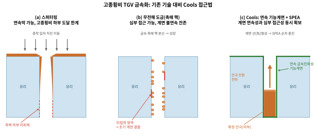
A TGV is a fine hole that runs vertically through a glass substrate to connect wiring on the top and bottom. In high-aspect-ratio TGVs, sputtering struggles to form a uniform film down to the lower sidewall, while wet electroless plating disperses metal catalyst nuclei and then grows them, which can leave unbonded areas.
Those unbonded areas act as initial interface defects where delamination begins under thermal cycling or damp-heat conditions. In advanced packaging, where a single large-area glass panel carries tens of thousands to hundreds of thousands of TGVs, localized interface defects determine overall yield and long-term reliability.
Cools addresses the problem with two technologies.
The first is an interface design that first converts the entire inner wall of the glass into a single continuous, metal-affinitive functional interface. Rather than attaching metal particles first, the method forms an uninterrupted metallizable interface across the whole via in advance.
The second is what the company calls a Self-Propagating Electrode Architecture (SPEA). SPEA places a fixed electrode only at the bottom of the via or in a specific region, and areas reached by the growing metal are sequentially converted into electrodes. Filling then proceeds from the bottom upward without the top of the via closing off first or seams and voids remaining inside.
"Glass core substrates and glass interposers differ in via size and wiring density, but the manufacturing principle is the same," Cho said. "In this presentation I will set out how to build a single TGV metallization platform that handles not just individual via plating but large-area panels at PLP scale."
Cools currently holds 118 patent applications filed with the Korean Intellectual Property Office related to glass substrate packaging. Its intellectual property portfolio covers the full glass substrate packaging process, including glass-metal bonding, continuous functional metallization interfaces, TGV seed formation, metal-ion-storing sidewalls, SPEA, sequential filling, and power feeding and redistribution layers for large-area panels.
Cools develops interface, bonding, metallization and thermal management technologies for advanced semiconductor packaging. It is taking part in programs including the 15th cohort of IBK Changgong Busan Center and the 5th cohort of KDB NextOne Busan.
Distributed via neta.